Google DeepMind bets on optical chips to accelerate frontier AI models
UK-US lab explores photonic interconnects to cut energy consumption and latency in training clusters for foundation models
Key Takeaways
- Photonic interconnects replace electrical pulses with light to transport data between accelerators
- Energy consumption of training clusters grows faster than the efficiency of conventional chips
- Google DeepMind maintains research on hardware architectures for large-scale foundation models
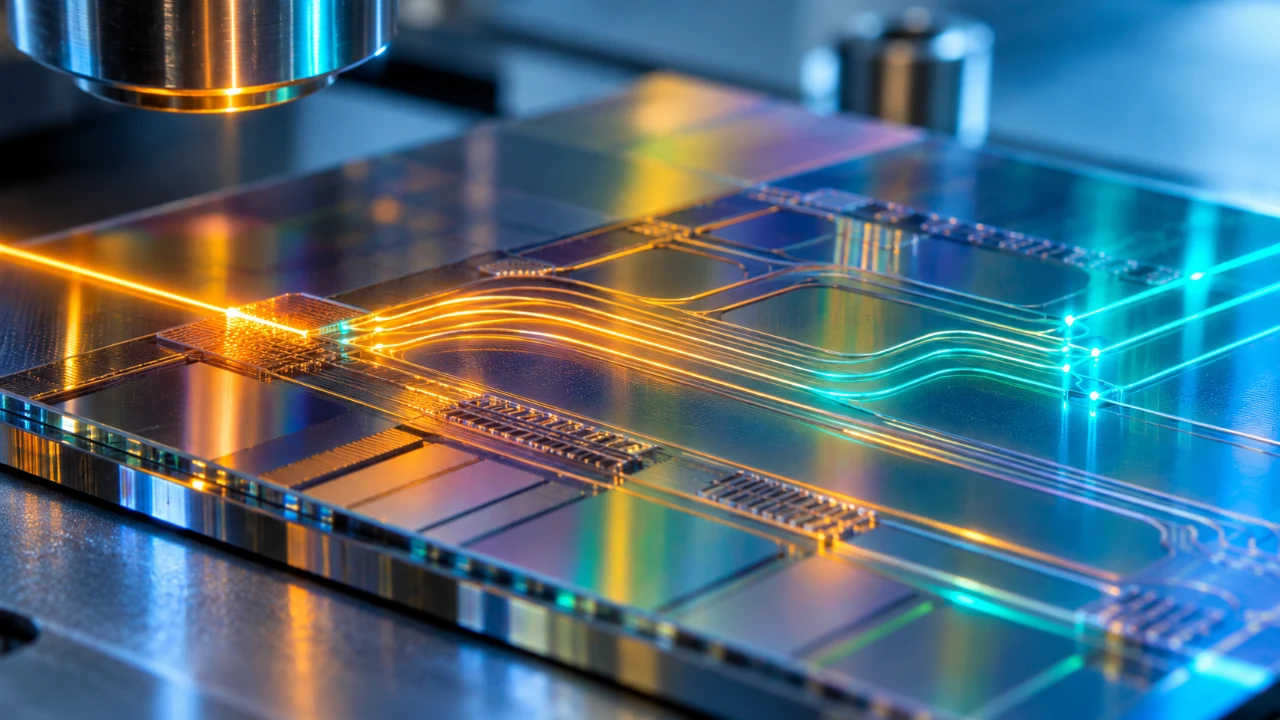
Google DeepMind is expanding research into photonic interconnects as a path to unlock the next performance leap in training clusters for frontier artificial intelligence models. The approach replaces traditional electrical pulses in copper with light signals transmitted through silicon waveguides, reducing latency and energy consumption in communication between accelerators.
The lab, based in the UK and the US, published the update on its official technology blog, signaling that infrastructure research remains a strategic front parallel to model development.
Why light matters
As foundation models grow in parameters, the bottleneck is no longer just the processing capacity of each chip but the speed at which thousands of accelerators exchange data with each other. Conventional electrical interconnects dissipate heat and impose physical limits on bandwidth.
Silicon photonics attacks exactly this point: by converting electrical signals into light within the chip itself, it is possible to transport larger volumes of data over longer distances with minimal energy loss. The concept, studied for years in academia, gains urgency with the scale of AI-dedicated datacenters.
What the bet reveals
DeepMind's move reinforces an industry trend: competition for frontier models has migrated to the physical layer. It is not enough to optimize algorithms—the hardware that supports them must be redesigned.
The lab did not detail production timelines or specific industrial partners in this update, keeping the announcement in the realm of applied research. Still, the signal is clear for the semiconductor sector: the integration of photonics and silicon should guide the next generation of AI infrastructure.
Practical impact
From a technical standpoint, optical interconnects could enable larger clusters without proportional growth in power consumption, addressing the main physical limiter of current training datacenters.
Operationally, adoption at scale depends on manufacturing maturity and cost per wafer—factors that will determine whether photonics moves from labs to production racks in the coming cycles.